Advanced Stackups

Multilayer PCB India

Complex multi-tiered substrate lamination engineered to support high-speed routing in space-constrained, performance-critical devices.

```
High-Density Engineering

Mastering Spatial Complexity with Precision Multilayer Stackups

When electronic form factors shrink while computing demands skyrocket, two dimensions are no longer enough. Multilayer printed circuit boards expand routing paths into the vertical axis, alternating layers of copper and insulating dielectric materials under high heat and immense pressure to build an integrated multi-tiered architectural network.

Historically, multi-layer designs were reserved only for extreme high-end mainframe computing. Today, they form the structural backbone of complex commercial hardware—from advanced smart-grid industrial controllers to complex automotive telematics blocks. Navigating multiple layers requires flawless core lamination and absolute layer registration to prevent hidden internal layout failures.
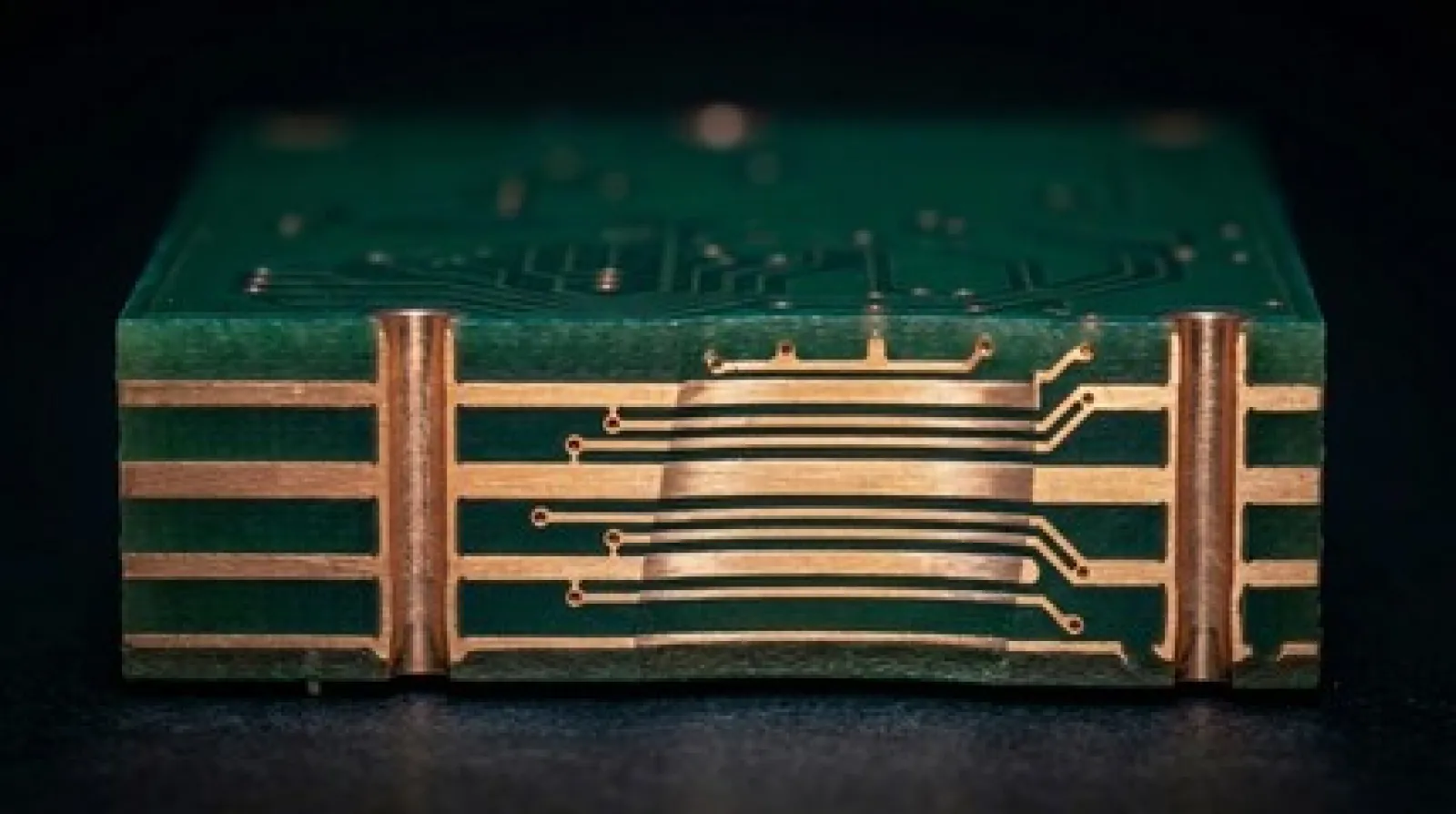
Complex Multi-layer PCB Inspection

Substrate Micro-Sectioning

Lamination analysis for high-density interconnect routing matrices.

The Subtle Physics of Internal Layers

Managing controlled impedance, signal path crossovers, and thermal stack pressures.

As signals cross between inner layers via blind or buried micro-vias, trace behavior transitions from basic electrical conduction to complex electromagnetic wave propagation. At high processing speeds, any mismatch in trace width, layer height, or substrate uniformity instantly creates an impedance shift, leading to signal degradation or data dropouts.

To counter this, our manufacturing framework balances structural core selection with raw prepreg resin flow during high-pressure thermal press sequences. By monitoring the dielectric thickness down to a single micron, we precisely anchor differential pair tracking parameters, preventing trace distortions from shifting internal signal return loops.

"In a multilayer environment, layer registration alignment determines product survival. A shift of just 20 microns between inner planes during thermal compression can sever via connections or cause permanent inner-layer shorts."

— Chemical Lamination Engineering Review

Critical Multilayer Architectural Pillars:

  • Controlled Impedance Modeling: Tight trace geometries matched perfectly to your target dielectric parameters (50 Ohm single-ended / 100 Ohm differential defaults).
  • Blind & Buried Vias: Laser-drilled interconnect options that skip entire layers entirely, preserving vital routing real estate on outer rows.

Sovereign Ecosystem Sourcing

Sourcing dense multilayer stackups from international vendors forces developers into long, blind iterations when resolving complex layout anomalies or layer stack imbalances.

At pcbmadeinindia.com, our local design review groups provide responsive, domestic validation. We parse complex multilayer files locally, executing comprehensive Design for Manufacturability (DFM) audits to intercept registration errors before copper panels touch the lamination press.

Direct Engineer Access Zero Import Customs Drag
Strategic Localization

Securing Critical Advanced Hardware Production Within Borders

Our multi-layer production systems are explicitly tailored to decouple Indian hardware innovators from long international turnaround gaps and unstable raw substrate access.

By coordinating high-grade lamination architectures within domestic frameworks, we safeguard your design layouts and keep critical intellectual properties protected. From custom prototypes to production-ready arrays, we blend physical process tracking with accessible engineering advice to give your project a clean launch.

Multilayer Capability Tolerances

Granular parameter limits for our advanced stackup lamination systems.

Parameter Definition Standard Range Advanced Limits
Layer Quantities 4 to 6 Layers Up to 12 Layers Max
Layer Registration Limits 3 mil (0.075mm) 1.5 mil (0.038mm)
Impedance Tolerances Plus or minus 10% Plus or minus 5%
Minimum Core Substrate 8 mil (0.2mm) 4 mil (0.1mm)
Max Finished Copper Weight 2 oz (Outer / Inner) Up to 4 oz Max
Lamination Thickness Profile 0.8mm to 1.6mm 0.4mm to 3.2mm

Note: Custom stackup configurations combining different dielectric constants or high-Tg requirements must be authorized with our engineering group prior to layout compilation.

Ready to Lock in Your Multilayer Stackup?

Bypass complex global supply lines. Send your multi-tier layout directories directly to our facility for quick lamination processing and extensive electrical diagnostic reviews.